Sony FY2021 Q3 Financial Report

EP&S
• Next is the Electronics Products & Solutions (“EP&S”) segment.
• Despite a favorable impact on sales from foreign exchange rates, Q3 sales decreased 2% year-on-year to 686.9 billion yen, primarily due to a decrease in the unit sales of our products resulting from a decline in stay-at-home demand and a shortage in the supply of components.
• Despite the favorable impact of foreign exchange rates and an improvement in product mix, operating income decreased 23.3 billion yen year-on-year to 80.0 billion yen, primarily due to the impact of the decrease in sales.
• FY21 sales are expected to increase 80 billion yen compared to our previous forecast to 2 trillion 360 billion yen and operating income is expected to increase 20 billion yen compared to our previous forecast to 210 billion yen.
• Operating income margin this fiscal year is expected to exceed 8%. The efforts we have been making to improve our profitability are steadily bearing fruit.

I&SS
• Next is the Imaging & Sensing Solutions (“I&SS”) segment.
• FY21 Q3 sales increased a significant 22% year-on-year to 324.8 billion yen, primarily due to an increase in sales of high-end image sensors for mobile products.
• Operating income increased 13.3 billion yen year-on-year to 64.7 billion yen, primarily due to the impact of the increase in sales.
• Our FY21 sales are expected to decrease 30 billion yen compared to our previous forecast to 1 trillion 70 billion yen.
• The FY21 operating income forecast remains unchanged from the previous forecast.

Posted in Financial results| Tagged , , | 1 Comment

Sony Killed The DSLR‽

The Art of Photography beat me to something I have been thinking about this year. Sony killed the DSLR and some people are having trouble accepting what Sony did. For those into technology, it was inevitable that mirrorless was going to kill the DSLR with so many exciting sensor technologies around the corner. The big one we were all waiting for and still are waiting for is a true global shutter, but the stacked image sensor, PDAF pixels, and BSI technology seems to have been enough to put the final nail in the DSLR coffin once and for all.

I for one will not miss the DSLR, because I honestly never owned one myself due to my dislike of the technology. I shot rangefinder before mirrorless and while I used a DSLR at work when I was forced to, I always hated the clunky DSLR experience so I am glad it will finally be replaced with a better thought-out design. Some thought this day would never come, but I was certain it would be coming sooner rather than later, and now that Canon and Nikon are done with DSLRs the rest of us should be too. Thank you, Sony for doing us all a massive favor and showing photographers that there is a better way to take photos even if it took some longer than others to accept.

Follow SonyAddict on FacebookTwitterInstagram, and YouTube

Plus our owners’ groups
Sony a1 Owners Group
Sony a9 Owners Group
Sony a7 Owners Group

Posted in Press releases| 1 Comment

Canadian Press Announces Sony As Exclusive Provider For Imaging Products


The Canadian Press Makes Sony Electronics its Exclusive Provider for Imaging Products
Canada’s Largest News Organization will outfit all journalists with Sony cameras and lenses

TORONTO, CANADA – January 31, 2022 – Sony Electronics, a global imaging leader, and The Canadian Press, Canada’s trusted national news agency, announced today that Sony would be the exclusive imaging products provider for the media company.

With more than 180 journalists, The Canadian Press produces real-time, bilingual multimedia news published by major digital, broadcast and print media. The switch to Sony will mean the photojournalists and videographers at The Canadian Press will use a variety of Sony cameras and lenses including the Sony Alpha 1 and Alpha 9 II products to quickly capture hundreds of powerful editorial photos and videos every day, ranging from large-scale global sporting events to local Canadian news, politics and lifestyle content.

“We are honored to announce this collaboration with The Canadian Press, a leader in delivering news and best-in-class multimedia content across Canada,” said Mark Saddleton, Sony Canada Country Head and Director of Sales. “The journalists at The Canadian Press have a front row seat for Canada’s biggest events across politics, sports and entertainment and we are delighted to support their visual storytelling.”

“Sony’s innovative technology takes the high quality of our visual journalism to a whole new level,” said Malcolm Kirk, President of The Canadian Press. “More than 600 media clients rely on our online CP Images archive as the go-to destination for contemporary and historic multimedia imagery of Canada’s people, places and events. That’s why we were looking for more than just a camera provider. We needed a true partner committed to helping us deliver first-rate visual journalism.”

“Sony’s commitment goes beyond providing lightweight equipment for handling fast action, hostile situations, and extreme weather conditions, without sacrificing image quality,” said Megan Leach, who manages visual journalists at The Canadian Press and heads up the planning and packaging department. “Our journalists truly appreciate how the silent camera performance allows them to stay behind the scenes, but more importantly, that Sony is responsive to our feedback.”

“From the outset, they’ve taken a relationship-driven approach to the upgrade, which will bring a unified look to our coverage since all our staff photographers and reporters will be shooting with the same brand of cameras for photos and videos for the first time “They understood the ongoing training and support was as critical as the technology. We’re thrilled to have their support as we expand our visual coverage and meet the future needs of our industry.”

The roll out of Sony imaging kits to Canadian Press journalists is already in progress, with distribution planned throughout early 2022.


About Sony Electronics Inc.
Sony Electronics is a subsidiary of Sony Corporation of America and an affiliate of Sony Group Corporation (Japan), one of the most comprehensive entertainment companies in the world, with a portfolio that encompasses electronics, music, motion pictures, mobile, gaming, robotics and financial services. Headquartered in San Diego, California, Sony Electronics is a leader in electronics for the consumer and professional markets. Operations include research and development, engineering, sales, marketing, distribution and customer service. Sony Electronics creates products that innovate and inspire generations, such as the award-winning Alpha Interchangeable Lens Cameras and revolutionary high-resolution audio products. Sony is also a leading manufacturer of end-to-end solutions from 4K professional broadcast and A/V equipment to industry leading 4K and 8K Ultra HD TVs. Visit http://www.sony.com/news for more information.

About The Canadian Press
The Canadian Press has been Canada’s trusted news leader for more than 100 years and is the exclusive Canadian distributor of international news from The Associated Press. More than 180 journalists produce, package and deliver real-time, bilingual news articles, photos, graphics, video and audio clips for use in newspapers, magazines, radio and TV newscasts, websites, company blogs, social channels, digital signage screens and more. Clients depend on their reliable, accurate and fast coverage, written and edited according to the standards set for the industry by The Canadian Press Stylebook. Through its commercial division, The Canadian Press also helps media, PR and marketing professionals by providing photography, videography and other custom content services; media monitoring, press release distribution and CP style training. http://www.thecanadianpress.com

via pixelshift

Posted in Press releases| Tagged | 4 Comments

Samyang AF 135mm f/1.8 FE Size Comparison vs Sony 135mm f/1.8 GM vs Sigma 135mm f/1.8


Samyang AF 135mm f/1.8 FE:
B&H Photo / Amazon / Adorama
Sigma 135mm F1.8 DG HSM:
B&H Photo / AmazonAdorama
Sony 135mm f/1.8 GM:
B&H Photo / Amazon / Adorama

The Samyang AF 135mm f/1.8 FE wasn’t announced long ago, but now camerasize.com has included it on their comparison tool and interestingly it is very similar in size to the Sony 135mm f/1.8 and Sigma 135mm f/1.8 DG DN without the lens hood. If you’re interested you can make your own comparison here.

Follow SonyAddict on FacebookTwitterInstagram, and YouTube

Plus our owners’ groups
Sony a1 Owners Group
Sony a9 Owners Group
Sony a7 Owners Group

Posted in 3rd Party Lens| Tagged , , , , , , , , , , , , , , , , , | 1 Comment

New Meyer-Optik Gorlitz Trioplan 35mm f/2.8 II Announced


Meyer-Optik Gorlitz Trioplan 35mm f/2.8 II:
B&H Photo / Adorama

Bad Kreuznach – 27th January 2022 – with the Trioplan 35 f2.8 II Meyer Optik Görlitz releases the third focal length of the famous Trioplan series. As of today – the sixth lens from Meyer Optik Görlitz can be ordered in the usual Meyer Optik mount versions.

“We are very pleased to now be able to introduce the Trioplan 35 II and are starting very positively into a new and hopefully more normal, year,” said Timo Heinze, Managing Director OPC Optics. “After we started with our new manufactory in Hamburg last quarter, the Trioplan 35 II is the first lens that will be manufactured there from the beginning.”

Popular Trioplan imaging language in the wide-angle range
The Trioplan 35 f2.8 II brings the famous Trioplan bokeh, also known as soap bubble bokeh, to the wide-angle range. This allows amazing effects to be created, especially at open aperture, giving your own images an individual artistic style and recognition value. Of course, when stopped down, the Trioplan 35 f2.8 II can also create quieter, particularly atmospheric images, flattering the main subject with a very softly drawn blur plane that almost looks painted. The compact 35mm focal length is of course perfect for use in reportage and street photography. At the same time, the short minimum object distance of 0.2 meters, despite the short focal length, allows it to be used in nature and portrait photography. Thus, the Trioplan 35 f2.8 II offers a high degree of versatility and a great deal of creative freedom.

High optical & mechanical quality for that Meyer is known for
The consistent implementation of the newly developed mechanical design, which all current lenses from Meyer Optik Görlitz have received, has of course also been continued in for new Trioplan 35 f2.8 II. The mechanical components from German manufacturers, the use of the best optical glass, which receives a specially developed coating and is manufactured in-house, the assembly by hand in our own factory and the individual testing of each lens, ensure the high quality & durability that distinguishes the lenses from Meyer Optik Görlitz.

Available for order now
Given the current circumstances (Corona, shortage of raw materials, etc.) and to be able to supply the desired lenses asap to as many customers as possible, the new Trioplan 35 II lenses are finalized based on the incoming orders. This means: The lenses are prepared as far as possible already and will finally be assembled to a definite version (e.g. Nikon F, Canon EF, Sony E, etc.) when a concrete order is placed. Although this results in a slightly longer delivery time (approx. three weeks from the order date), over/under production is avoided and thus demand can be fulfilled more precisely.

The Trioplan 35 II can be ordered now, for the first time also as a native version for Nikon Z and Canon RF, at https://www.meyer-optik-goerlitz.com/en/lenses/trioplan-35-f2.8-ii.

What follows?
Two true classics, the Biotar 58 f1.5 II and the Biotar 75 f1.5 II, are currently in series production and will expand the portfolio in this spring. Likewise, the other existing lenses will be successively expanded to include variants for Nikon Z and Canon RF. In parallel, new lenses are in planning / development and will be released later this year.

Posted in 3rd Party Lens| Tagged , , | 1 Comment

Sony Stacked CMOS Sensors


Sony’s Representative Inventions Supporting Stacked Multi-Functional CMOS Image Sensors

  • Sony Corporation
  • Sony Semiconductor Solutions Corporation

Taku Umebayashi, an employee of Sony, was awarded the Purple Ribbon Medal in the 2020 Spring Conferment of Medals of Honor. The Purple Ribbon Medals honor influential characters with their outstanding achievement in inventions and discoveries in the field of science and technology, and in the academic, sports, and arts and cultural fields. The medal was awarded to Mr. Umebayashi in appreciation to his achievement in the development of stacked multi-functional CMOS image sensors. His achievement in research and development had already received the Prime Minister Award of the National Commendation for Invention in 2016, and also with recommendation from the Japan Institute of Invention and Innovation (“JIII”), he received the Awards for Science and Technology (Development Category) of the Commendation for Science and Technology by the Minister of Education, Culture, Sports, Science and Technology in 2018. JIII had also recommended Mr. Umebayashi for the Purple Ribbon Medals.

Provided below are explanations of stacked multi-functional CMOS image sensors and Sony’s notable inventions which support them.

1. About Stacked CMOS Image Sensors
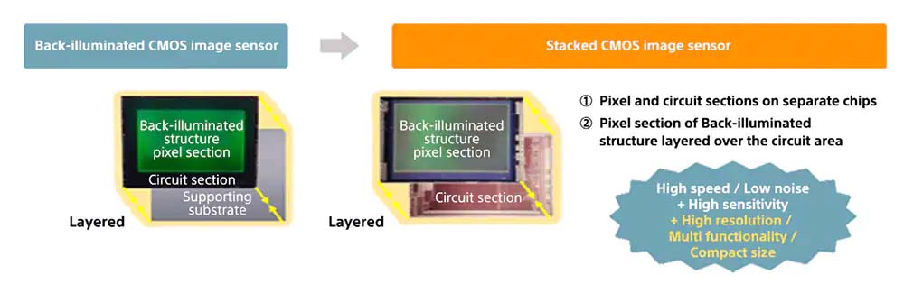
CMOS image sensors, also called “electronic eyes”, are a semiconductor core component that converts light into electronic information. They are often known for its use in smartphone cameras, but are also widely used as a key component in various areas such as for security cameras, automatic driving of vehicles, industrial applications such as factory automation, and medical applications. Such wide variety of use also requires a wide variety of functions. In conventional CMOS image sensors, a pixel section that performs photoelectric conversion and a signal processing circuit section are formed on the same silicon substrate, therefore it was impossible to increase the circuit size for multi-functionalization and to miniaturize the structure at the same time.

To overcome these technological challenges, a new approach was taken where the pixel section and the signal processing circuit section were formed on two separate silicon substrates respectively, and the two silicon substrates are aligned and bonded with high precision, and are connected electrically at multiple points (Japanese Patent Number 5773379 Taku Umebayashi, Hiroshi Takahashi, Reijiro Shoji). As a result, this allowed a wide signal processing area to be secured directly under the pixel part, and miniaturization and multi-functionalization to be achieved at the same time without impairing the high-quality performance that back-illuminated CMOS image sensors already had. The “one-story” silicon semiconductor device was changed to “two-stories”. This technology was mass-produced and commercialized for the first time in the world as stacked multi-functional CMOS image sensors. Smartphone cameras of recent years can support various imaging scenes, and have dramatically improved not only in image quality, but also in functionality and operability. It is no exaggeration to say that stacked CMOS image sensors contributed to these benefits greatly. In recent years, many products that utilize this technology have been produced as digital cameras used not only in smartphones but also in various electronic devices.


2. Sony Representative Inventions Supporting Stacked CMOS Image Sensors

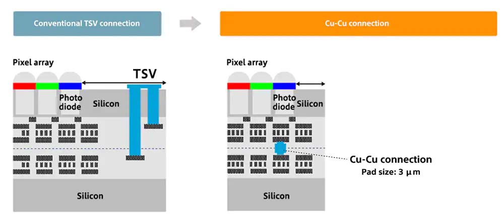
Cu-Cu Connections Adopted in Stacked CMOS Image Sensors
Sony has developed technologies that involve direct connections with Cu pads formed on the layering surfaces of pixel chips and logic circuit chips (e.g. the same patent above). Since this will not require electrical connection portion that penetrates the pixel chip, the connecting areas can be removed, and therefore, the image sensors can be made smaller with high productivity. Offering greater freedom in pin layout and high densification, this technology will contribute to development of stacked CMOS image sensors with broader and higher functions in the future.

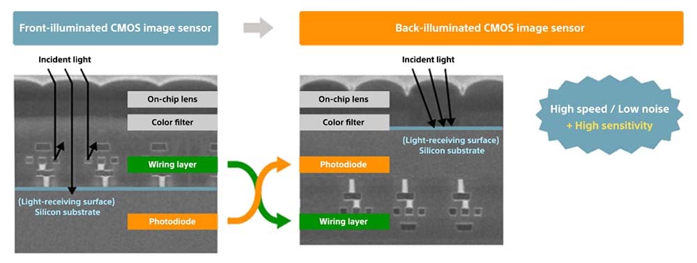
Back-Illuminated CMOS Image Sensors Suitable for Being Stacked with Logic Circuit Chip
A back-illuminated structure minimizes the degradation of sensitivity caused by different optical angle, while also increasing the amount of light that enters each pixel due to the lack of obstacles such as metal wiring and transistors that have been moved to the other side of the silicon substrate. However, compared to the conventional front-illuminated structures, the back-illuminated structures generally cause problems that result from its device structure and manufacturing process, such as noise, dark current, defective pixels, or color mixture, that lead to image degradation and also cause decrease in the signal-to-noise ratio.

To overcome this, Sony has developed a unique photo-diode structure (e.g. Japanese Patent Number 3759435 Ryoji Suzuki, Keiji Mabuchi, Tomonori Mori), that achieves higher sensitivity and lower random noise by reducing noise, dark current and defect pixels. Additionally, Sony’s advanced technologies such as high-precision alignment have addressed color mixture problems.

Pinned Photodiode Adopted for Back-Illuminated CMOS Image Sensors
The history of Sony’s inventions of image sensors goes back to the CCD era. Above all, Pinned Photodiode is a technology that contributes to improving the performance of back-illuminated CMOS image sensors, and the history of inventions and product development are as below.

In 1975, Sony invented a CCD image sensor that adopted a back-illuminated N+NP+N junction type and an N+NP+NP junction type Pinned Photodiode (PPD) (Japanese patent application number 1975-127646, 1975-127647 Yoshiaki Hagiwara). In the same year, inspired by such structure, Sony invented a PNP junction type PPD with VOD (vertical overflow drain) function (Japanese Patent No. 1215101 Yoshiaki Hagiwara). After that, Sony succeeded in making a principle prototype of a frame transfer CCD image sensor that adopted the PNP junction type PPD technology, having a high-impurity-concentration P+ channel stop region formed near a light receiving section by ion implantation technology for the first time in the world, and its technical paper was presented at the academic conference, SSDM 1978 (Y. Hagiwara, M. Abe, and C. Okada, “A 380H x 488V CCD imager with narrow channel transfer gates”, Proc. The 10th Conference on Solid State Devices, Tokyo, (1978)). In 1980, Sony succeeded in making a camera integrated VTR which incorporated a one-chip frame transfer CCD image sensor that adopted the PNP junction type PPD. President Iwama in Tokyo, Chairperson Morita in New York, at the time held a press conference respectively on the same day, which surprised the world. In 1987, Sony succeeded in developing a 8 mm video camcorder that adopted, for the first time in the world, the interline transfer CCD image sensor, which incorporated “PPD having a high-impurity-concentration P+ channel stop region formed near the light receiving section by ion implantation technology” with VOD function, and became the pioneer of the video camera market. The PPD technology that has been nurtured through such a long history is still used in back-illuminated CMOS image sensors.

3. Future Outlook
Stacked CMOS image sensors have made it possible to add completely new functions to CMOS image sensors themselves and have contributed to the dramatic expansion of the image sensor market. As a result, it has promoted domestic investment in equipment for mass production of image sensors and has invigorated the Japanese semiconductor industry.

In the coming era of IoT and AI technology, stacked multi-functional CMOS image sensors will play a large role as a platform for imaging devices that support a new era, and many products equipped with this technology are expected to make our lives richer and more convenient, and to make great contributions to the development and improvement of social infrastructure.

Posted in Press releases| Tagged , , | 2 Comments