Sony’s Representative Inventions Supporting Stacked Multi-Functional CMOS Image Sensors
- Sony Corporation
- Sony Semiconductor Solutions Corporation
Taku Umebayashi, an employee of Sony, was awarded the Purple Ribbon Medal in the 2020 Spring Conferment of Medals of Honor. The Purple Ribbon Medals honor influential characters with their outstanding achievement in inventions and discoveries in the field of science and technology, and in the academic, sports, and arts and cultural fields. The medal was awarded to Mr. Umebayashi in appreciation to his achievement in the development of stacked multi-functional CMOS image sensors. His achievement in research and development had already received the Prime Minister Award of the National Commendation for Invention in 2016, and also with recommendation from the Japan Institute of Invention and Innovation (“JIII”), he received the Awards for Science and Technology (Development Category) of the Commendation for Science and Technology by the Minister of Education, Culture, Sports, Science and Technology in 2018. JIII had also recommended Mr. Umebayashi for the Purple Ribbon Medals.
Provided below are explanations of stacked multi-functional CMOS image sensors and Sony’s notable inventions which support them.
1. About Stacked CMOS Image Sensors
CMOS image sensors, also called “electronic eyes”, are a semiconductor core component that converts light into electronic information. They are often known for its use in smartphone cameras, but are also widely used as a key component in various areas such as for security cameras, automatic driving of vehicles, industrial applications such as factory automation, and medical applications. Such wide variety of use also requires a wide variety of functions. In conventional CMOS image sensors, a pixel section that performs photoelectric conversion and a signal processing circuit section are formed on the same silicon substrate, therefore it was impossible to increase the circuit size for multi-functionalization and to miniaturize the structure at the same time.
To overcome these technological challenges, a new approach was taken where the pixel section and the signal processing circuit section were formed on two separate silicon substrates respectively, and the two silicon substrates are aligned and bonded with high precision, and are connected electrically at multiple points (Japanese Patent Number 5773379 Taku Umebayashi, Hiroshi Takahashi, Reijiro Shoji). As a result, this allowed a wide signal processing area to be secured directly under the pixel part, and miniaturization and multi-functionalization to be achieved at the same time without impairing the high-quality performance that back-illuminated CMOS image sensors already had. The “one-story” silicon semiconductor device was changed to “two-stories”. This technology was mass-produced and commercialized for the first time in the world as stacked multi-functional CMOS image sensors. Smartphone cameras of recent years can support various imaging scenes, and have dramatically improved not only in image quality, but also in functionality and operability. It is no exaggeration to say that stacked CMOS image sensors contributed to these benefits greatly. In recent years, many products that utilize this technology have been produced as digital cameras used not only in smartphones but also in various electronic devices.

2. Sony Representative Inventions Supporting Stacked CMOS Image Sensors
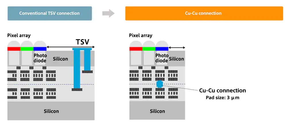
Cu-Cu Connections Adopted in Stacked CMOS Image Sensors
Sony has developed technologies that involve direct connections with Cu pads formed on the layering surfaces of pixel chips and logic circuit chips (e.g. the same patent above). Since this will not require electrical connection portion that penetrates the pixel chip, the connecting areas can be removed, and therefore, the image sensors can be made smaller with high productivity. Offering greater freedom in pin layout and high densification, this technology will contribute to development of stacked CMOS image sensors with broader and higher functions in the future.

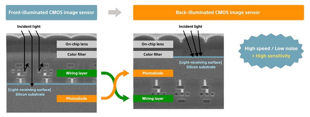
Back-Illuminated CMOS Image Sensors Suitable for Being Stacked with Logic Circuit Chip
A back-illuminated structure minimizes the degradation of sensitivity caused by different optical angle, while also increasing the amount of light that enters each pixel due to the lack of obstacles such as metal wiring and transistors that have been moved to the other side of the silicon substrate. However, compared to the conventional front-illuminated structures, the back-illuminated structures generally cause problems that result from its device structure and manufacturing process, such as noise, dark current, defective pixels, or color mixture, that lead to image degradation and also cause decrease in the signal-to-noise ratio.
To overcome this, Sony has developed a unique photo-diode structure (e.g. Japanese Patent Number 3759435 Ryoji Suzuki, Keiji Mabuchi, Tomonori Mori), that achieves higher sensitivity and lower random noise by reducing noise, dark current and defect pixels. Additionally, Sony’s advanced technologies such as high-precision alignment have addressed color mixture problems.

Pinned Photodiode Adopted for Back-Illuminated CMOS Image Sensors
The history of Sony’s inventions of image sensors goes back to the CCD era. Above all, Pinned Photodiode is a technology that contributes to improving the performance of back-illuminated CMOS image sensors, and the history of inventions and product development are as below.
In 1975, Sony invented a CCD image sensor that adopted a back-illuminated N+NP+N junction type and an N+NP+NP junction type Pinned Photodiode (PPD) (Japanese patent application number 1975-127646, 1975-127647 Yoshiaki Hagiwara). In the same year, inspired by such structure, Sony invented a PNP junction type PPD with VOD (vertical overflow drain) function (Japanese Patent No. 1215101 Yoshiaki Hagiwara). After that, Sony succeeded in making a principle prototype of a frame transfer CCD image sensor that adopted the PNP junction type PPD technology, having a high-impurity-concentration P+ channel stop region formed near a light receiving section by ion implantation technology for the first time in the world, and its technical paper was presented at the academic conference, SSDM 1978 (Y. Hagiwara, M. Abe, and C. Okada, “A 380H x 488V CCD imager with narrow channel transfer gates”, Proc. The 10th Conference on Solid State Devices, Tokyo, (1978)). In 1980, Sony succeeded in making a camera integrated VTR which incorporated a one-chip frame transfer CCD image sensor that adopted the PNP junction type PPD. President Iwama in Tokyo, Chairperson Morita in New York, at the time held a press conference respectively on the same day, which surprised the world. In 1987, Sony succeeded in developing a 8 mm video camcorder that adopted, for the first time in the world, the interline transfer CCD image sensor, which incorporated “PPD having a high-impurity-concentration P+ channel stop region formed near the light receiving section by ion implantation technology” with VOD function, and became the pioneer of the video camera market. The PPD technology that has been nurtured through such a long history is still used in back-illuminated CMOS image sensors.
3. Future Outlook
Stacked CMOS image sensors have made it possible to add completely new functions to CMOS image sensors themselves and have contributed to the dramatic expansion of the image sensor market. As a result, it has promoted domestic investment in equipment for mass production of image sensors and has invigorated the Japanese semiconductor industry.
In the coming era of IoT and AI technology, stacked multi-functional CMOS image sensors will play a large role as a platform for imaging devices that support a new era, and many products equipped with this technology are expected to make our lives richer and more convenient, and to make great contributions to the development and improvement of social infrastructure.