Image courtesy of image-resource
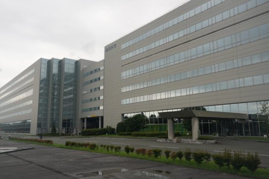
Imaging-resource went inside Sony Kumamoto after the earthquake and received unprecedented access. Previously IR released footage of the quake and cleanup effort, which you can view here, but today they released one of many follow-up stories to come. Below are the key points.
- Photos from the article were hand picked by Sony
- “There’s a better than 50% chance that the sensor in your current camera came out of this factory.”
- Sony grows its silicon and silicon wafers are sliced from massive, single crystals of silicon
- “finished wafers are about 12 inches (300 mm) in diameter, by perhaps 4 to 6 feet long (1.4 – 2 meters)”
- The process of growing a crystal of silicon is kind of like rock candy
- “In the early 1970s, 3-inch wafers were standard, now 12-inch (300mm) wafers are commonplace, and manufacturers continue working to increase sizes even further.”
- The article covers at length the cleaning process of the silicon entering the Kumamoto facility and how it goes from a class 1000 (1000 particles larger than 0.5 microns per cubic foot of air) to class 1 (1 particle larger than 0.5 microns in size per cubic foot of air) clean room, which involved a purified water cleaning as the first step.
- The factory is almost completely automated, with people mainly servicing machines.
- Humans are just too inconsistent and dirty for this kind of work.
- The air flow in these rooms is massive to suck any particles down through the floor.
- When they cut the chips apart they use a 20-30 microns thick (0.02-0.03 mm or just 0.008-0.012 inches) thin-kerf diamond saw, and it spins at 30,000 – 60,000 rpm to minimize damage to the sensor and keep the blade rigid.
- After they are cut Sony assembles the chip with whatever electronics it might need extremely quickly to create the package for camera manufacturers.
- Then Sony tests their chips to ensure they meet specifications before getting them ready to ship out
If you are interested in learning more about these points you can read the entire Imaging-resource article here.
 Image courtesy of image-resource