


Nikkeibp wrote an article about the DRAM that Sony embedded in their sensor to make cameras like the Sony a9 possible and advancements necessary to make it happen are interesting. I was going to take the time to make bullet points of it, but Image-sensors-world beat me to it with a very concise list of the most important things:
The processing flow is:
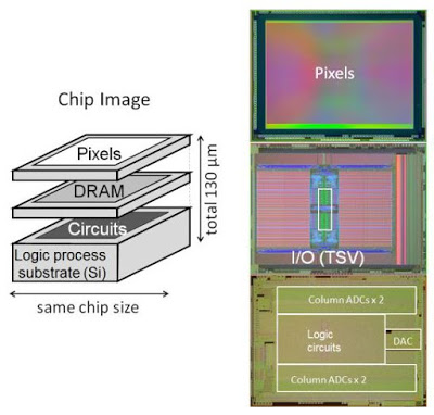
- The pixel, DRAM and logic wafers are manufactured using 90nm, 30nm and 40nm processes, respectively.
- The DRAM wafer and the logic wafer are joined together, and the thickness of the DRAM wafer is reduced to 3μm
- The DRAM and logic wafers are electrically connected with TSVs
- The stacked wafers of the DRAM and logic are joined to the pixel wafer
- The 3-layer wafer stack is thinned down to 130um and connected with TSVs
The numbers of TSVs connecting the pixel layer with DRAM is ~15,000 and DRAM with logic layer is ~20,000. Both of the TSVs have a diameter of 2.5μm and a pitch of 6.3μm. The 1/2.3-inch sensor has a resolution of 21.3MP and pixel size of 1.22um.
Via image-sensors-world and Nikkeibp

